Reducing the contact resistance in 2D semiconducting transistors
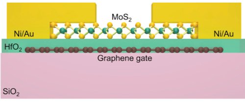
Device structure
2D transition-metal dichalcogenides (TMDs) such as molybdenum disulphide (MoS2) could be ideal for making next-generation optoelectronics devices. Those made from the materials so far suffer from low ON-currents, however, because of the large contact resistance between the metal electrodes in the devices and the TMDs. Researchers in the US, Korea and Singapore have now overcome this problem and have made high-performance field-effect transistors from monolayer MoS2 films containing graphene bottom gates that are one atom thick.
The devices boast a low contact resistance of just 2.3 kΩ·μm between the MoS2 and electrodes made from nickel, have excellent switching characteristics and a high channel conductance (of more than 100 μS/μm). They also have short channel lengths and a fully transparent channel region which means that they might be useful for various optoelectronics applications such as biosensors, photodetectors, and display backplanes.
Transition-metal dichalcogenides
MoS2 is a single-layer material and belongs to the family of TMDs. These are quasi-two-dimensional materials with the chemical formula MX2, consisting of an atomic plane of a transition metal M (Ti, Nb, Mo, Re) sandwiched between the atomic planes of a chalcogen X (S, Se or Te). TMDs go from being indirect bandgap semiconductors in the bulk to direct bandgap semiconductors when scaled down to monolayer thickness. These monolayers efficiently absorb and emit light and so might find use in a variety of electronics and optoelectronics device applications.
There is a problem, however, in that the ON-current in transistors fabricated from 2D semiconductors thus far has been considerably lower than that of silicon devices. This is because it is difficult to reduce both the contact resistance and channel length in devices made from atomically thin materials.
Cleaner and flatter graphene surface
The new MoS2-based FET was made by James Hone of Columbia University in New York and colleagues at the US Army Research Laboratory in Maryland, Nanjing University in China, Sungkyunkwan University in Suwon, Korea, and Nanyang Technological University in Singapore. It consists of a monolayer MoS2 channel contacted by nickel/gold metal electrodes atop a monolayer graphene back-gate with a high-k dielectric layer.
The graphene was grown by chemical vapour deposition on copper foil and then electrochemically delaminated onto an oxidized silicon substrate. The delamination step is quicker and cheaper than conventional wet-etching transfer techniques and has the added advantage of producing a substrate that contains fewer impurities when it is adhered to graphene, thus making for a cleaner and flatter graphene surface.
Advertisement
The single-atom thick graphene also shrinks the height of the gate electrode and its smooth surface is ideal for growing ultrathin high-quality dielectric layers. The graphene gate can then be used to highly dope the monolayer MoS2, to a carrier density of 4.6 x 1013cm-2. This allows the researchers to control the electrostatic properties of the contact region between the MoS2 and the nickel electrode, which is how they can reduce the contact resistance down to just 2.3 kΩ·μm in this region.
Short channel lengths
Hone and colleagues made devices with channel lengths as short as 50 and 14 nm with a 5-nm-sized gate dielectric that have excellent switching characteristics – including a near-ideal subthreshold slope of 64 millivolts per decade, low threshold voltage (of around 0.5 V) and a high channel conductance (of more than 100 μS/μm). The fact that the graphene gate makes the device highly transparent on flexible polymer substrates means that it might be used in a host of flexible optoelectronics applications too.
To summarize, reduced contact resistance improves both the device’s switching characteristics and reduces its ON-state current to levels close to those defined by the International Technology Roadmap for Semiconductors (ITRS), say the researchers. “Thanks to the enhanced electrostatic gating effect, we found no significant degradation in the device’s performance upon scaling the channel length down to 14 nm. Our work thus provides a chemical-free, energy-friendly, and scalable method of achieving high doping levels of 2D materials, which may benefit device fabrication.”