How to Create Schematic and PCB Libs in EasyEDA
What Will I Learn?
The users will learn the following:
- You will learn how to create your own schematic libs (library) in EasyEDA.
- You will learn how to create your own PCB libs (library) in EasyEDA.
- You will learn how to check your created schematic and PCB libs (library) if workable.
Requirements
For you to follow, you are required to have;
- EasyEDA Circuit Simulator and PCB Design (go to www.easyeda.com and run the software on your web browser)
- Internet connection (EasyEDA is a web-base software; you will need internet to run the software)
- Laptop or PC
Difficulty
- Intermediate
Tutorial Contents
Description
This Tutorial is about on how to create schematic and PCB libs in EasyEDA. Creating schematic and PCB libs is very essential and I'm glad to know that EasyEDA has this feature. It can be use when there is no available lib for your component. That is the time you need to create your own lib for your component.
For this tutorial, I will create schematic and PCB lib for 74LS04 IC. It is an inverter IC.
Opening EasyEDA
Step 1
go to www.easyeda.com to open their simulator.
.
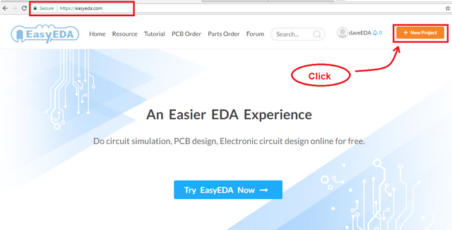
Step 2
Click the "New Project" to load their editor.
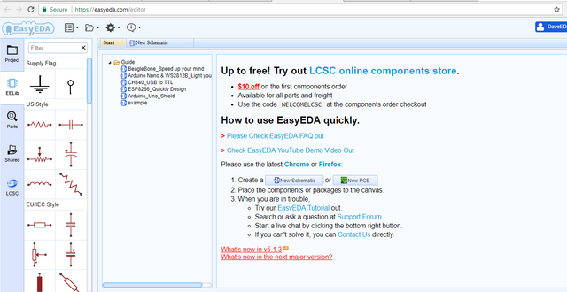
This is the EasyEDA editor.
Part A | Creating Schematic Lib
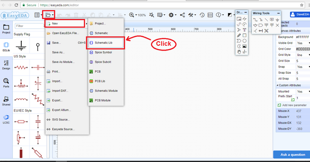
Step 1 | Schematic Lib Tab
To start creating lib, Click "folder" icon, go to "new" and click "schematic lib".
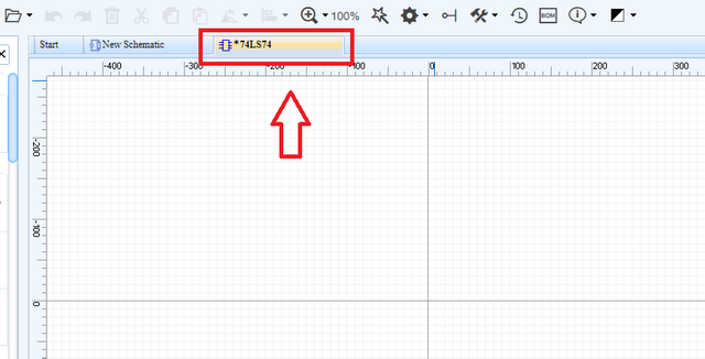
Step 2
Fill out the "Manufacturer Part Number" and click "Ok"
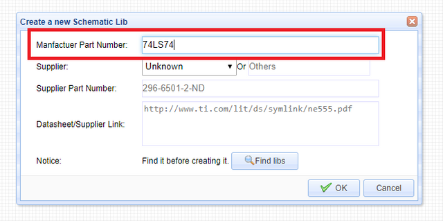
We will now see a new Tab for schematic lib and named it "74LS04".
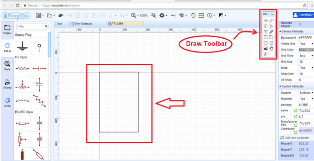
Step 3 | Drawing Layout
Draw a rectangle from draw toolbar. We use rectangle because 74LS04 is a 14-pin IC and in rectangular form.
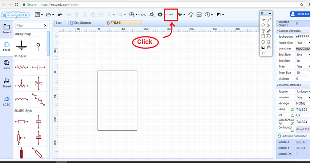
Step 4 | Inserting Pins
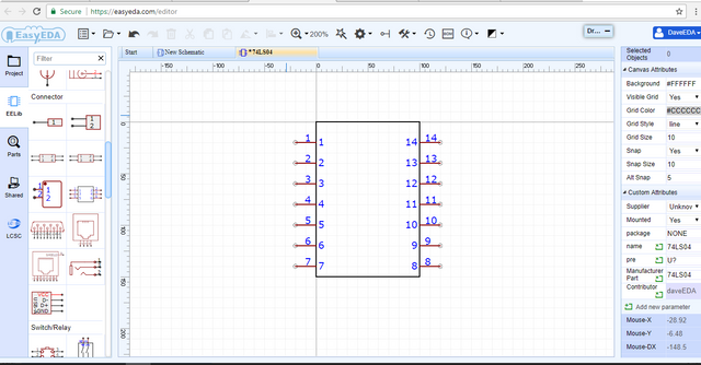
74LS04 is a 14-pin IC, so we need to put 14 pins at sides of the rectangle. Click "Place Pin" button.
Start putting pins. The circle part of the pins 
must be put in a way that it is away from the rectangle. Use "R" or "space" of your keyboard to rotate the pins.
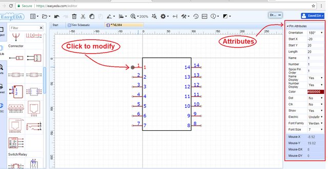
Step 5 | Modifying Attributes to the Pins
After inserting the pins, you can apply or modify its attributes. Click the pin you want to modify and pin attributes panel will appear.
I am changing the pin names to match with pin configuration of 74LS04. This is the pin configuration of 74LS04.
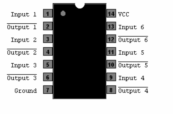
74LS04
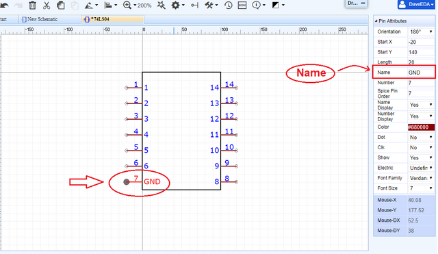
I will change the name of pin 7 to "GND or ground", this pin will be allocated for ground.
Now, let us change the pins' names to its appropriate pin configuration.
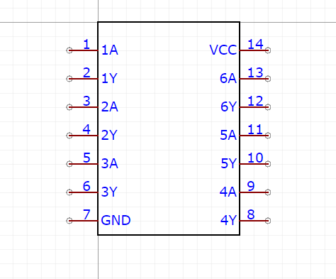
Here are the names of symbols to fully understand.
1A - Input 1
1Y - Output 1
2A - Input 2
2Y - Output 2
3A - Input 3
3Y - Output 3
GND - Ground
VCC - Supply Voltage
6A - Input 6
6Y - Output 6
5A - Input 5
5Y - Output 5
4A - Input 4
4Y - Output 4
Step 5 | Naming the component
To name the component, just add "text" command from our drawing toolbar. Press "R" and "space" to change orientation.
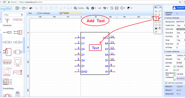
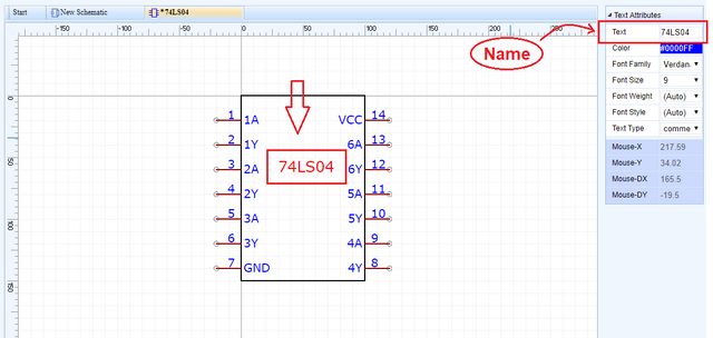
And then, Click the "text" to change its name on attribute panel.
Step 6 | Saving
To save, choose first the packing of our 74LS04. Packaging will be our actual appearance of IC.
You click the drawn schematic and click the "package" attribute. A dialog box for selecting package will appear. Because it is a 14-pin IC, we wil choose the S0IC-14 package.
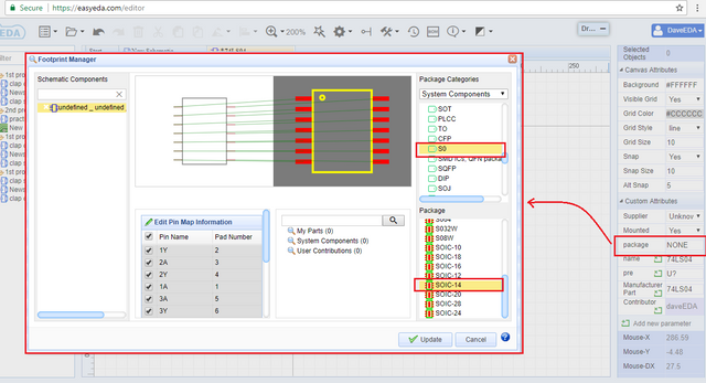
And then, Press Update.
To save, click the "folder" icon and select "save as"
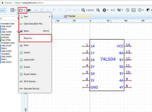
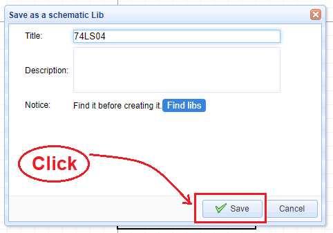
Click "save" to add this to our Library.
Part B| Creating PCB Lib
Step 1 | PCB Lib Tab
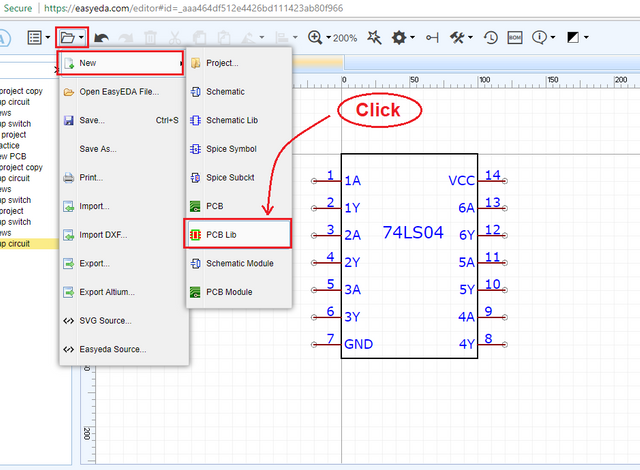
To start, Click the "folder" icon, select "new" and click "PCB Lib"
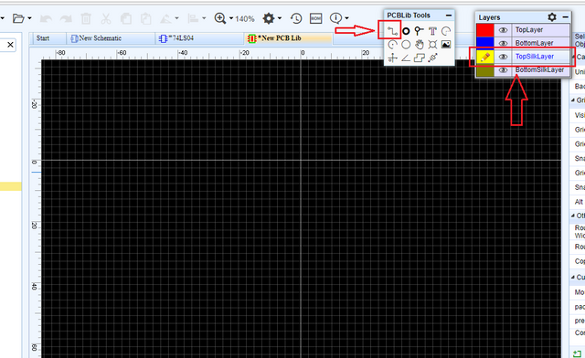
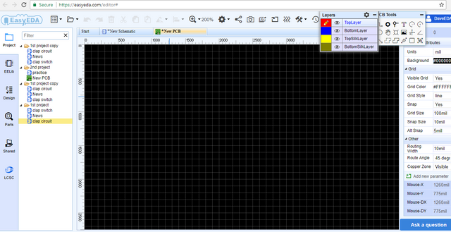
The working area will change to "PCB Lib" with a black background.
Step 2 | Drawing the Layout
To draw the layout, locate the "PCB Lib Tools" toolbar and click the "track" command. Also change the layer to "TopSilkLayer", colored yellow.
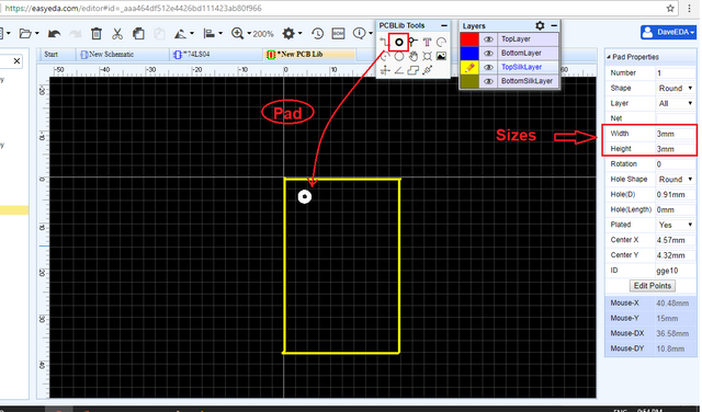
Using the "track" command, draw a rectangle and add a pad to our rectangle. "Pad" command can be found in our "PCB Lib Tools". This pad will determine the location of our pin 1. Usually pin 1 is beside the pad. To change the height and width of our drawn layer, just look in to our attribute panel and change the sizes.
Step 3 | Drawing the Pins
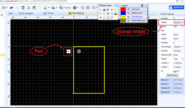
We will use the "Pad" command to draw our pins. We will change the shape of pad to rectangle to form pins.
Let us resize the pad to make it exactly same us the pins.
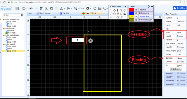
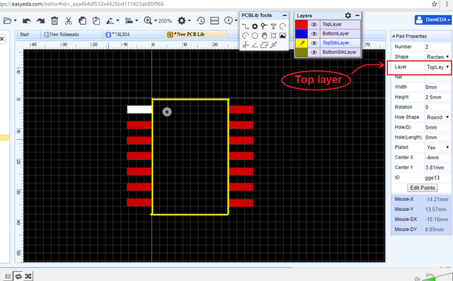
Now, Copy the pin and put all the 14 pins at the side of our rectangle. Change the pin's layer to "TopLayer".
Step 4 | Saving
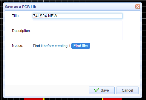
To save our create PCB lib, click the "folder" icon, select "save as".
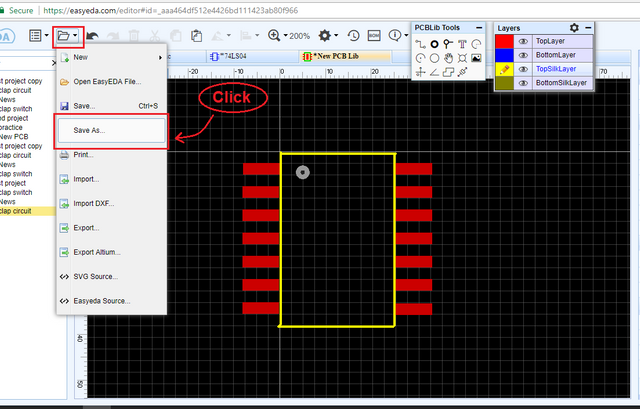
Let us put name on it and click save.
Alright, our PCB lib for 74LS04 is now finished.
Part C | Checking our Work
Step 1 | Check Schematic Lib
To try, we will open a new schematic project an check if our created schematic Lib is workable.
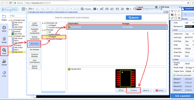
We will click the "Parts"button, go to "My Parts" (it is where our created parts will be saved).
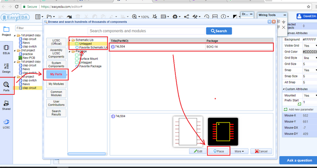
So, we can see that our created part is available. We will click "Place" button and see if it can put to our schematic work station.
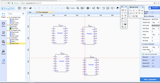
Therefore, our created schematic is good and working.
Step 2 | Check PCB Lib
We will open the PCB design workstation. Go to "folder" icon, select"new" and click "PCB".
We will click again the "Parts" button to place our PCB lib, select "My Parts" and look for our created lib and click "Place".
And we see that our created lib is place.
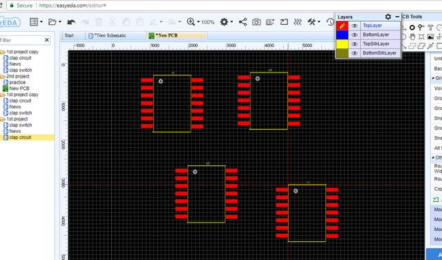
Therefore, our created PCB Lib is good and workable.
Curriculum
Here is my another tutorial, you can check it out. This could might help you.
Posted on Utopian.io - Rewarding Open Source Contributors
Thank you for the contribution. It has been approved.
You can contact us on Discord.
[utopian-moderator]
Hey @thinkingmind I am @utopian-io. I have just upvoted you!
Achievements
Suggestions
Get Noticed!
Community-Driven Witness!
I am the first and only Steem Community-Driven Witness. Participate on Discord. Lets GROW TOGETHER!
Up-vote this comment to grow my power and help Open Source contributions like this one. Want to chat? Join me on Discord https://discord.gg/Pc8HG9x