A Review Of 2-D Material FETs: Graphene and Beyond Graphene...
Imagine that you can climb into space on a thin staircase. Or you'll have a phone or TV that you can never break. Moreover, this phone or TV, light as hair, ultra thin and you can stretch as much as you want. Get a smart dress that will instantly detect vital items such as blood pressure, pulse, blood sugar level. In addition, this dress is too thin to be seen by the eye and wrap your entire body. But even so, you will not be cold. You'll be able to change the pattern, color, and anything you want, just by pressing a button at a time. Here is the magic material: Two Dimensional Material.
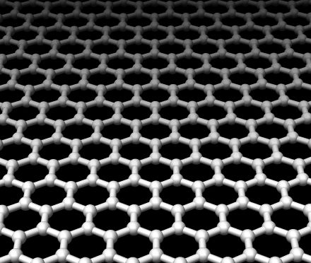
The backbone of today's semiconductor electronics is the field effect transistors. It is the basic building block of modern information and communication technology and applications for the defense industry. Progress in these issues depends on the rapid development of the performance of the field-effect transistors. Another option to achieve this goal is to adopt the new "channel-materials”to field-effect transistors. The rise of two-dimensional materials was achieved by the successful preparation of graphene samples in 2004. In particular, the observed high carrier mobilities increased the expectation that graphene was an excellent channel material for field-effect transistors. Thus, graphene would be the heir of the traditional semiconductors. However, it was later realized that graphene could not fully meet these high expectations. This is because there is no band gap which is absolutely necessary for the proper operation of a field effect transistor.
wikimedia commons
That bad news about graphene was a factor that causes the community to lose its interests. Later, the publication of an article describing the fabrication of a single-layer MoS2 domain-effect transistor began to accelerate research on two-dimensional materials. In a surprisingly short time, all classes of new two-dimensional materials were discovered. Increasingly globally, research groups are currently working on two-dimensional field-effect transistors.
Transition Metal Dichalcogenide Transistor was firstly produced in 2011. This transistor is a MOSFET with a 500nm gate with a single-layer. It has a MoS2 channel and obtained by exfoliation method. Thanks to the MoS2 having a bandwidth of approximately 2 eV, this device showed good switching performances and a good on/off ratio with a voltage swing of 4V. Then the other groups also fabricated MOSFETs with single-layer and multi-layer MoS2 channels. In most cases, MoS2 synthesized by the exfoliation method. Also reported is the use of CVD-grown MoS2. Recently, in addition to single transistors, simple electronic circuits using MoS2 MOSFETs were also available.
MoS2 is a stretchable and a flexible material, it is very attractive for flexible electronics. MOSFETs can be produced on MOS2 based substrates. Although experimental studies on transition metal dicalcogenides transistors have focused on MoS2 MOSFETs, it has been proven in the past that the first single or multi-layered WSe2 MOSFETs can also be realized.
You first have to synthesize the 2 dimensional material for producing your transistors. It is better that they have uniform thicknesses with high crystallographic quality as large-area sheets. The van der Waals materials can be formed by the exfoliation method. The superimposed layers of the material are connected to each other with van Der Waals bonds. Those van Der Waals bonds are molecular and very easy to break. Mechanical exfoliation is frequently used to synthesize graphene, transition metal dichalcogenides, and phosphorene layers. This approach is simple and does not require expensive equipment, but is time-consuming. However, only limited and very small size flakes can be obtained. The liquid exfoliation method is another exfoliation method in which two-dimensional flakes dispersed in a liquid are present. This method is quite effective, but the scattered flakes are small, thus making the transistor and circuit process challenging.
In addition, ultrahigh precision gas detectors can be fabricated with field effect transistors using two-dimensional materials. The gas sensors that can be made in this way are classified as conductive sensors. The sensing mechanism of the conductive sensors is based on the transfer of charge between the sensor layer and the material that is chemically adsorbed to the surface. A charge transfer in this way affects the electrical resistance of the sensitive material and the sensor response occurs.
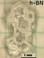
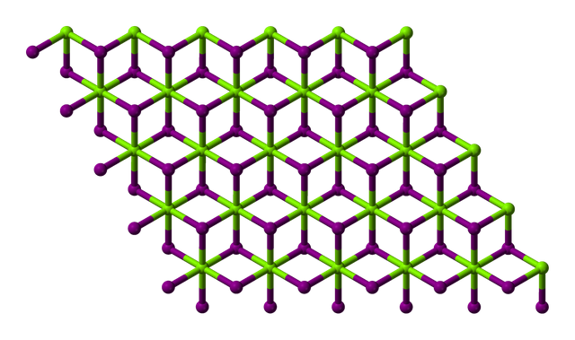
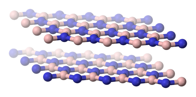
A standard definition of two-dimensional materials is available to all. There is an ISO terminology standard for this. If you would like to see the detailed definition. Please see ISO / TS 80004-13: 2017: Graphene and related two-dimensional (2D) materials. The 2-D Nanomaterials which are discovered after graphene are called Beyond Graphene 2-D materials. If we look at its features: Hexagonal boron nitride, h-BN has a large band gap in the UV region of the spectrum and is resistant to mechanical and chemical interactions. Dielectric strength is high. For example, electric fields can meet up to 0.8 V / nm. It is used for use as a substrate or for encapsulation for two-dimensional devices. For instance, when combined with graphene, h-BN contributes to the increase of mobility of graphene devices very well. These materials have very high dielectric strength. They are therefore known as gate dielectric and/or tunnel barriers.
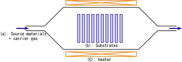
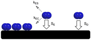
Growth/coating process of two-dimensional materials is the first and main step of production. For this reason, it is the step that attracts the most attention. There are many publications reporting MoS2 and other two-dimensional materials using a powder precursor in a furnace. The techniques based on metal organic precursors such as MOCVD and ALD can be a more attractive alternative than the growth techniques used in the furnace. The optimization of film properties made in this manner is at a more critical level in the advancement of this technology. Two important factors to be aware of in this technique are how to affect the stress of the substrate and the resulting film.

The so-called "Scotch tape" adhesive tape technique is the easiest and most cost-effective mechanical peeling method used in material synthesis. It has a much less damaging effect than other methods. In addition, however, it allows wide monolayer flakes to be obtained on different substrates. The non-carbon two-dimensional materials obtained by this method are transition metal dichalcogenides and hexagonal boron nitride. This method is very cost-effective but restricts the production of large quantities of materials. Alternative ways of synthesizing non-carbonic two-dimensional materials are also available. They depend on the type of application and the nature of the desired material. Chemical exfoliation method can be given as an example.
![Carbophiliac [Public domain], via Wikimedia Commons](https://upload.wikimedia.org/wikipedia/commons/2/26/Graphene_xyz.jpg)
![State of the art [Public domain], from Wikimedia Commons](https://upload.wikimedia.org/wikipedia/commons/6/66/Wiki_kisliuk_n2-tungsten.JPG)
![Hexagonal Boron Nitride NIMSoffice [Public domain], from Wikimedia Commons](https://upload.wikimedia.org/wikipedia/commons/b/bc/Hbncrystals.jpg)
![S-kei [Public domain], from Wikimedia Commons](https://upload.wikimedia.org/wikipedia/commons/9/9e/ThermalCVD.PNG)
![Donmike10 (talk) at en.wikipedia. [Public domain], from Wikimedia Commons](https://upload.wikimedia.org/wikipedia/commons/d/d7/Tape_dispenser.JPG)
![Arnero [Public domain], from Wikimedia Commons](https://upload.wikimedia.org/wikipedia/commons/7/79/Carbon_nanorim_zigzag_povray.PNG)
With this method, the crystalline material is dispersed in a solvent with a suitable surface tension. Transition metal dichalcogenides and hexagonal boron nitride can be synthesized by this method. In addition, an atom or molecule insertion method can be used. In this method, it is also possible to place molecules or atoms in/between the compounds in the layered structure, such as transition metal dichalcogenide or hexagonal boron nitride. Another method is surface growth. With this method, the materials are deposited onto the substrate. Single-element nanoplates, such as silicene, are frequently synthesized by this method using metallic substrates. In another method called solution phase amplification, a two-dimensional material having a very precise thickness can be produced in a flat state. In this way, colloidal syntheses of transition metal dichalcogenides such as TiS2, VS2, ZrS2, HfS2, NbS2, TaS2, TiSe2, VSe2 and NbSe2 are made. Another growth for synthesis is the vapor deposition (CVD) method. This method is a non-catalytic process for transition metal dichalcogenides. Another method associated with this method is large scale CVD. This method is often used to enlarge graphene in very large areas.
References
- 2 Dimensional Materials
- Single-layer MoS2 transistors
- Nanomaterials and Nanoscience
- Silicene field-effect transistors operating at room temperature
If you’re in the field of science, technology, engineering, or mathematics, you can join SteemSTEM community in the discord:

The link below is the discord channel of StemQ :

Note that; all images used in this post are free for commercial use, they are royalty-free with the links to original images provided under them
Congratulations,
you just received a 11.66% upvote from @steemhq - Community Bot!
Wanna join and receive free upvotes yourself?

Vote for
steemhq.witnesson Steemit or directly on SteemConnect and join the Community Witness.This service was brought to you by SteemHQ.com