Nanoelectronics : The Growing Developments Of Nanotechnology

The field of electronics, which deals with the development of technological and physical bases for the construction of integrated electronic circuits with element sizes less than 100 nanometers, is called nanoelectronics. The very term "nanoelectronics" reflects the transition from microelectronics of modern semiconductors, where the dimensions of the elements are measured by units of micrometers, to smaller elements - tens of nanometers in size.
With the transition to nanoscale, quantum effects start to dominate in the schemes, which open up a lot of new properties, and, accordingly, signify the prospects of their useful use. And if for quantum electronics microelectronics often remained parasitic, because, for example, with a decrease in the size of the transistor, the tunneling effect begins to interfere with its work, then nanoelectronics on the contrary - is intended to use such effects as a basis for nanoheterostructural electronics.

Each of us uses electronics daily, and for sure many people already notice some unambiguous trends. Memory in computers is increasing, processors are becoming more productive, the size of devices is decreasing. What is the reason for this?
In the first place - with the change in the physical dimensions of the elements of the microcircuits, from which all electronic devices are essentially built. Although the physics of the processes remains approximately the same today, the size of the devices is getting smaller and smaller. A large semiconductor device operates slower and consumes more energy, and a nanotransistor works faster and consumes less energy.
It is known that all material bodies consist of atoms. And why would not electronics reach atomic scale? This new field of electronics will solve such problems, which on an ordinary silicon base are simply impossible to solve in principle.
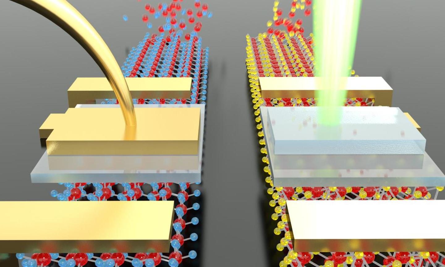
Of great interest now is graphene and similar monolayer materials (see article - Unexpected properties of the usual carbon). Such materials in one atom of thickness have remarkable properties that can be combined to create various electronic circuits.
For example, technologies related to probe microscopy make it possible to build various structures of individual atoms on the surface of a conductor in an ultrahigh vacuum, simply rearranging them. What is not the basis for creating monatomic electronic devices?
Nanoelectronics and electronics
Manipulations of matter at the molecular level have already affected many industries, and they did not bypass electronics. Microprocessors and integrated circuits are built just like this. Leading countries are investing in the further development of this technological path - for the transition to the nanoscale to occur faster, wider, and improve further.
Some successes, by the way already achieved. Intel said in 2007 that a processor based on a 45nm structural element was developed (submitted by VIA Nano) and the next step would reach 5 nm. IBM is going to achieve 9 nm thanks to graphene.

Carbon nanotubes (graphene) - one of the most promising nanomaterials for electronics. They allow not only to reduce the size of transistors, but also to give the electronics truly revolutionary properties, both mechanical and optical. Nanotubes do not retain light, are mobile, they retain the electronic properties of circuits.
Particularly creative optimists are already looking forward to the creation of portable computers that can be taken out of the pocket like a newspaper, or worn as a bracelet on the hand, and if desired, as the newspaper is deployed, and the entire computer will be like a fold-out high-resolution touch screen of paper thickness.

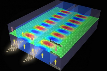
Another perspective for the application of nanotechnology and the use of nanomaterials is the development and creation of new generation hard drives. Albert Firth and Peter Grunberg in 2007 received the Nobel Prize for the discovery of the quantum-mechanical effect of ultrahigh magnetic resistance (GMR effect), when thin films of metal from alternating conducting and ferromagnetic layers significantly change their magnetic resistance when the mutual direction of magnetization changes.
By controlling the magnetization of the structure by means of an external magnetic field, it is possible to create so accurate magnetic field sensors and to perform such an accurate recording on the storage medium that its storage density will reach the atomic level.
Did not pass nanoelectronics and plasmatronic. Collective vibrations of free electrons within a metal have a characteristic plasmon resonance wavelength of about 400 nm (for a silver particle 50 nm in size). The development of nanoplasmonics, it can be said, began in 2000, when progress in improving nanoparticle technology was accelerated.
It turned out that an electromagnetic wave can be transmitted along a chain of metallic nanoparticles, exciting plasmon oscillations. Such a technology will allow us to integrate into the computer hardware logical chains that are able to work much faster and to transmit more information than traditional optical systems, and the systems will be much smaller than the optical ones.
Leaders in the field of nanoelectronics, and electronics in general, today are Taiwan, South Korea, Singapore, China, Germany, England and France.
The most modern electronics are produced today in the US, and the most massive producer of high-tech electronics is Taiwan, thanks to the investments of Japanese and American companies.
China is a traditional leader in budget electronics, but here the situation is gradually changing: cheap labor attracts investors from high-tech companies that plan to establish their own nanotechnologies in China.
US and many European countries have a good potential. The base in the field of microwave, radiative structures, photodetectors, solar batteries and power electronics allows in principle to create nanotechnology nanotechnologies and develop them.
This potential requires economic conditions and organization for carrying out fundamental research and scientific development. All the rest is: a technological base, promising personnel and a scientific qualified environment. Only large investments are needed, and this often turns out to be an Achilles heel ...
One example of the application of nanotechnology: Nanoantennes for obtaining solar energy.

References for Text and Images:
- https://www.rmit.edu.au/research/research-institutes-centres-and-groups/research-groups/functional-materials-and-microsystems/projects/nanoelectronic-and-nanophotonic-structures
- https://www.livescience.com/topics/nanotechnology
- https://www.livescience.com/topics/nanotechnology
- http://www.ohgizmo.com/2008/01/31/new-highly-efficient-solar-panels-could-work-day-and-night/
- https://www.nanowerk.com/nanotechnology-news/newsid%3D39269.php
- http://www.ohgizmo.com/2008/01/31/new-highly-efficient-solar-panels-could-work-day-and-night/
Support @steemstem and the #steemstem
project - curating and supporting quality STEM
related content on Steemit

For more information, click here!!!!
Send minimum 0.100 SBD to bid for votes.
Do you know, you can also earn daily passive income simply by delegating your Steem Power to @minnowhelper by clicking following links: 10SP, 100SP, 500SP, 1000SP or Another amount. (10 SP minimum)
This post has received a 0.31 % upvote from @booster thanks to: @chotho.
Nice post.good job.this pst recive 0.60% upvote. @masud90